The Facility
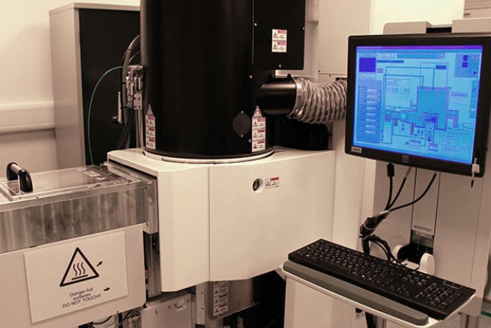
We deliver nanofabrication services through the James Watt Nanofabrication Centre (JWNC) in Glasgow, UK. The facility opened in 2006 and has since benefited from a series of expansions taking it from a 750 m2 space to 1400 m2. The facility went through a further expansion in 2020 to accommodate an additional electron beam lithography tool. The cleanroom facility spans three floors with an extensive tool set that is frequently updated and enhanced to improve capability.

Our Four Key Process Areas
Lithography
For defining features in the range 20nm to ~cm; we have two commercial 8” electron beam lithography tools, two contact photolithography systems and a nanoimprint lithography tool. A wealth of expertise in process optimisation and resist technology provides you the necessary patterning technology to meet your application needs.
Example photonic structures include gratings for DFB lasers, diffractive optical elements, waveguides and plasmonic filters.

Plasma Processing
Comprehensive dry etching and deposition capabilities enabling a broad range of material processing. The dry etch facility contains 5 RIE, 6 ICP systems tuned to etch materials such as silicon, dielectrics, III-Vs, II-VIs, metals, polymers and physically hard materials such as diamond and SiC. Materials such as silicon nitride, silicon oxide and metal oxides can also be deposited as thin films. We can often apply existing processes from our extensive recipe database, and also optimise parameters to provide the necessary geometries you require.
Example quantum devices include microfabricated ion traps, MOT gratings and lasers tuned to atomic transitions.

Metallisation
A suite of fully automated load-locked electron beam evaporation tools and multi-target sputtering systems. Common metals deposited by evaporation include Au, Ti, Pd, Pt, Al, Ge, Ni and NiCr. The tools allow additional flexibility in film formation with in-situ plasma treatments, substrate temperature control, sample rotation and tilt for feature side-wall coating.
Example components include electrodes for piezo electric systems, MEMS electrostatically driven actuators and microfluidic channel systems.

Characterisation and Metrology
The facility houses a variety of metrology systems suitable to characterise devices dimensionally, chemically and electrically. This includes access to three high resolution scanning electron microscopes, energy dispersive x-ray analysis, atomic force microscopy, three surface profilometers, scanning ellipsometry, electrical probe stations and numerous optical microscopes.
Example geometries include optical grating structures for head-up displays, nanogap platforms for single molecule electronics and MEMS gravimeters.

Equipment and Capability
We are keen to learn about your applications and technical challenges and how we might use our expertise and experience to satisfy your micro and nanofabrication needs. We are constantly improving our tool set and processes so if you cannot find what you are looking for, please contact us to discuss your requirements.
Nanofabrication Facility
Kelvin Nanotechnology works within 1400 m2 of zoned cleanroom suite (James Watt Nanofabrication Centre) spanning 24 rooms on three levels with lithography tools and scanning electron microscopy facilities at ground level. The column room for the Raith EBPG5200 lithography tool (continually maintained at ±0.1°C) is class 10, four rooms are class 10,000 and the remainder are class 1000. Each room has an assigned activity such as photolithography or metallisation. There are 32 laminar air flow cabinets each dedicated to specific tasks, for example substrate cleaning. Equipment and process reliability are maintained through service contracts and quality assurance.
Lithography
E-Beam Lithography (Nanobeam nB5, Raith EBPG5200) – Two commercial tools: Max. wafer size 200 mm with full stage travel. Field size up to 1 mm. Operating at 80 or 100 keV. Up to 125 MHz pattern generation. Z-stage accommodating large range of substrate thicknesses. Direct write stitching accuracy of < 5 nm and 0.46 nm rms layer-to-layer alignment. Demonstrated single lines down to < 5 nm using HSQ resist. Full service contracts.
Photolithography (SUSS MicroTec MA6/BA6, MA8/BA8) – Max. wafer size: 200 mm. Top and back side alignment function. Proximity, hard and vacuum contact modes. UV exposure optics and i-line/g-line filters. Chucks for bond alignment and silicon fusion applications.
Nanoimprint Lithography (EVG 6200NT) – Max. wafer size: 200 mm. Feature sizes down to 20 nm, ≤1 μm alignment optics. Fully automated computer controlled imprinting cycles and graphical data logging. In-house production of stamps to a max. size: 200 mm.
Plasma Processing and Etching
Reactive Ion Etching (5 machines including Oxford Instruments System 100 & 80 plus) – Processing of silicon-based materials (Si, poly Si, SiO₂, quartz, Si₃N₄, SiGe), metals (Al, Au, Co, Fe, Ge, NiFe, Pd, Pt, Ti). III-V materials (GaAs, AlGaAs, AlGaN, GaN, high-K, low damage nitride), III-V materials with In (InP, InGaAs, InGaAsP, AlInAs), II-VI materials (CdTe, ZnSe), polymers, sapphire and LiNbO₃. Process gases include: Ar, CH₄, CHF₃, CF₄, C₂F₆, H₂, N₂, O₂, SF₆, SiCl₄ and SiF₄. Optional sample stage heating and etch depth monitoring interferometry.
Inductive Coupled Plasma RIE (Oxford Instruments PlasmaPro 100 Estrelas, STS ICP RIE, SPTS Rapier) – Processing of SiGe, Ge and deep Si Bosch/mixed/cryogenic process etching. Process gases include: Ar, C₄F₈, He, N₂, O₂ and SF₆. (Oxford Instruments System 100 ICP 180 & PlasmaPro 100 Cobra) – processing of III-V materials (AlGaAs, AlGaN, GaAs, GaN, InGaAs, InP, high-K, low damage nitride) and metals (Al, Au, Pd, Pt and Ti) etching. Process gases include: Ar, BCl₃, CF₄, CH₄, Cl₂, H₂, HBr, He, N₂, O₂, SF₆ and SiCl₄. Optional sample stage heating and etch depth monitoring interferometry. (SPTS APS Synapse) – Deep SiO₂ etching up to 1um/min.
Focussed Ion Beam (FEI Nova 200) – A dual beam SEM / focussed ion beam system for sample cross sectioning and preparation. In-chamber micromanipulation and Pt and W deposition capability.
Wet Etching – a large range of chemical etching and cleaning processes including HF, piranha and RCA. Thermostatically controlled wet etching baths for silicon micromachining with alkaline solutions and many selective metal, dielectric and III-V material etches.
Metallisation and Deposition
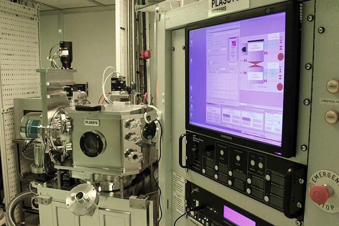
E-Beam Evaporation (2×Plassys MEB 550S) – Al, Au, Ge, Mo, Ni, NiCr, Pd, Pt and Ti deposition on sample ≤ 150 mm. Substrate tilt, planetary motion, temperature control and preparation by O₂ plasma and Ar ion etch.
Thermal Evaporation (Plassys MEB 400) – Broad range of metals and metal oxides available deposited within a box coater system or diffusion pumped bell jar chamber containing 6 thermal sources with ceramic and tungsten boats.
Sputter Coating (Plassys MP 900S) – Al, Cu, Co, Cr, Gd, TaN, Ti, W, WTi, V deposition with DC and/or RF magnetrons on samples ≤ 100 mm. Substrate double planetary motion and reactive sputtering.
PECVD (Oxford Instruments System 100 & 80 plus, SPTS Delta) – Deposition of SiO₂, Si₃N₄, amorphous Si and low stress Si₃N₄. Process gases include: CF₄ & O₂ mix, He, N₂O, N₂, NH₃ and SiH₄.
Thermal Oxidation (AVT PEO 601) – Dry thermal SiO₂ and SiOₓN₁-x growth up to 1100°C. Ramp rates up to 100°C/min for a wafer batch or 20°C/s for single wafers. The system can take 25 off 100 mm diameter wafers. Gases include: O₂, N₂O, N₂ and forming gas. Alternative systems for wet oxidation are available.
Characterisation
Scanning Electron Microscopy (FEI Nova NanoSEM 630) – Max. substrate size: 200 mm. Ultra high resolution imaging under high (1.0 nm at 15 kV) and low vacuum (1.8 nm at 3 kV). Non-conducting substrates can be imaged without coatings. Backscatter and secondary electron detection. (Hitachi S-4700 SEM) – Max. substrate size: 150 mm. 1.5 nm resolution at 15 kV, accelerating voltages from 0.5 to 30 kV, high resolution back scattered detector. Critical dimension measurement and energy dispersive x-ray (EDX) analysis tools. (Hitachi SU8240) – Max. substrate size: 200 mm. 0.8 nm resolution at 15 kV, EDX.
Atomic Force Microscopy (Bruker Dimension Icon) – Max. substrate size: 200 mm diameter and 15 mm thick, z-range of 10 μm, x-y imaging area of 90 μm. Drift rate <0.2 nm/min., vertical noise <30 pm. PeakForce TUNA nanoelectrical mapping.
Profilometry (Veeco Dektak 6M Stylus Profiler & Bruker Dektak XT Stylus Profiler) – Surface morphology, step height and stress analysis. Max. substrate size: 200 mm diameter and 50 mm thick, vertical resolution 0.01 nm at 6500 nm range. Z range up to 1 mm, x-y stage translation of 150×150 mm. (Brucker Contour GT-X 3D Optical Surface Profiler) – Max. substrate size: 200mm. Vertical measurement range up to 10 mm, vertical resolution down to 0.05 nm, step height repeatability < 0.1%. Built-in self-calibration.
Ellipsometry – used to establish the thickness, index, loss index and roughness of thin films.
Optical Microscopy – a range of microscopes covering light field, dark field and Nomarski imaging modes with image capture facilities. x-y dimensional measurement capability.
