Electron Beam Foundry
Kelvin Nanotechnology has over twenty years’ experience in electron beam lithography and nanofabrication. Electron beam lithography provides a route to versatile nano-patterning for a vast range of applications. Single or multi-level patterns can be written onto almost any type of substrate then transferred by etching or depositing metals, insulators, biocompatible materials, optical or electronic layers.
Our core technology is based around an electron beam lithography suite containing Nanobeam nB5 and Raith EBPG5200 commercial tools. Features from 20 nm can be written easily and quickly on up to 200 mm wafers. Full industrial service contracts ensure 96% up time and with over 50,000 samples written in the last ten years, this high utility translates into cost effective manufacturing.
We specialise in high resolution, large area, multi-level electron beam lithography for photonics, quantum technologies and telecoms industries. Applications include devices such as laser gratings, transistor gates, imprint masks, optical elements, photonic crystals, nanotextured surfaces and many more.
This depth of experience at KNT is central to our ability to translate your needs to high resolution patterning.


We provide cost effective nanolithography with a 24-7 operation across three commercial EBL tools working at nm to mm length scales.
‘Pure-play’ E-Beam Foundry – customer supplied designs produced on a variety of substrate materials.
High resolution – feature sizes start at 20 nm with the capability to form sub-10 nm nanogaps.
Large area writing – cm sized patterns
Multi-level processing – level to level registration better than 15 nm (standard) or 1 nm (special) achieved using custom marker recognition software.
High throughput – rapid load/unload process by team of technicians has enabled >50,000 wafers written in last 10 years.
Up to 200mm diameter wafers – cassette exchange system enables multiple wafers to be written sequentially.
Extensive process database – covering the processing of semiconductors, dielectrics, metals and polymers.
Excellent cost-to-yield – from process setup and optimisation to Live wafer writing.
Application expertise – multi-discipline technical team with over 20 years’ experience spanning semiconductor, optoelectronics, nanoelectronics, quantum and bioelectronics sectors.

Tracks, channels or linear electrodes can be defined.

Raised dots or wells from 20 nm upwards can be formed in a variety of materials over large areas

Specialists in laser grating lithography and etch methods.

3D lithography used for wafer scale fabricated scanning thermal probes capable of resolving 0.1 mK temperature changes with 100 nm spatial resolution.

Compact, easily configured approach to cooling atoms in a magneto optical trap.
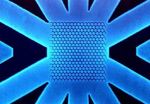
Two-dimensional photonic-bandgap structures.
