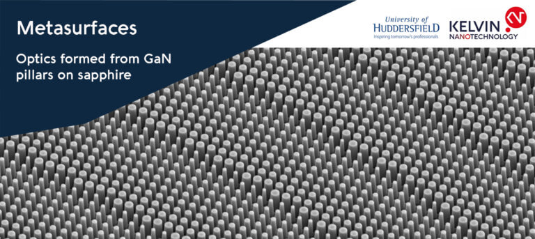
Metasurfaces have revolutionized the definition of compact optics. Using subwavelength periodic structures of nanostructured dielectrics, the refractive index and absorption properties of metasurfaces – which are 2D metamaterials – can manipulate light to a degree not possible with conventional bulk glasses and crystals. The phase, polarization, spin (for circularly polarized light), amplitude and wavelength of light can all be manipulated and crafted to user-specified values to mimic the action of a lens, which we refer to as a metalens (ML). MLs have four major advantages over traditional refractive lenses – superior resolution, lighter weight, miniaturization and cost. Many metasurfaces with useful functionalities have been proposed in recent years, yet although novel in their approach have few real-world applications. One such market is the use within infrared laser systems, such as laser designators. In this work, we demonstrate metasurface lenses working at a wavelength of λ = 1064 nm, with aperture d = 1 mm and four different Fnumbers (focal length f = 0.5, 1, 2 and 5 mm). The lenses are composed of 700 nm high a-Si pillars – ranging from 70- 360 nm diameter – which are fabricated using electron beam lithography (EBL) and reactive ion etching processes, on top of a fused silica substrate. Such lenses are shown to have diffraction-limited performance, with focal spot-size agreeing with theoretical values of λ‧f/d. Furthermore, we have designed large area lenses with aperture d = 10 mm, where the number of pillars per lens exceeds 550 million. By using an efficient Python script, we are able to produce these 100 mm2 samples with just 14 hours of EBL writing time.
Mitchell Kenney; James Grant; Danni Hao; Kevin Docherty; Gordon Mills; Graham Jeffrey; Donald Macleod; David Henry; Peter MacKay; Marc Sorel; Robert A. Lamb; David R. S. Cumming


